- 您现在的位置:买卖IC网 > Sheet目录337 > LT3003EMSE#TRPBF (Linear Technology)IC LED DRIVER BALLASTER 10-MSOP
LT3003
PIN FUNCTIONS
V EE (Pin 10): Lower Rail.
? Boost: Connect to System Ground
? Buck Mode: Connect to Inductor
? Buck-Boost Mode: Connect to Input Supply
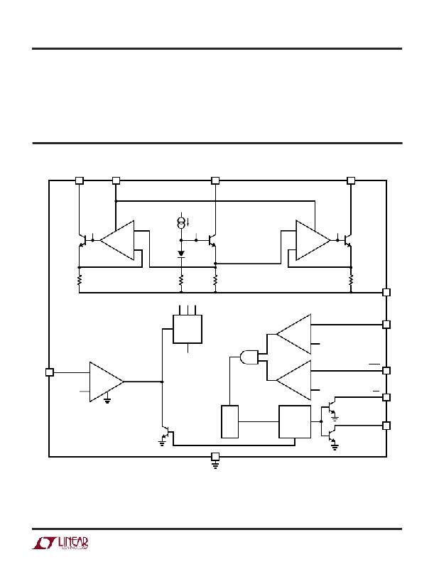
BLOCK DIAGRAM
Exposed Pad (Pin 11): GND. The ground for the IC should
be soldered to a continuous copper ground plane under
the LT3003 die. Soldering the Exposed Pad to the copper
ground plane under the device will reduce thermal resis-
tance and increase the power capability of the LT3003.
1
LED1
4
V MAX
2
LED2
3
LED3
V IN
B1
+
B2
+
B3
–
–
B1 B2 B3
V EE
10
PWM
+
V IN
5
LOGIC
V EE
–
3V
6
PWM
+
+
SHDN
9
0.5V
–
–
0.7V
OT1
7
BIAS
THERMAL
SHUTDOWN
BG
BG
125 ° C
OT2
8
150 ° C
11
EXPOSED PAD
3003 F01
Figure 1. Block Diagram
3003fa
5
发布紧急采购,3分钟左右您将得到回复。
相关PDF资料
LT3465AES6#TRMPBF
IC LED DRIVR WHITE BCKLGT TSOT-6
LT3466EDD-1#PBF
IC LED DRIVR WHITE BCKLGT 10-DFN
LT3466EDD#PBF
IC LED DRIVR WHITE BCKLGT 10-DFN
LT3474IFE#PBF
IC LED DRVR HP CONS CURR 16TSSOP
LT3475EFE-1#PBF
IC LED DRVR HP CONS CURR 20TSSOP
LT3476EUHF#PBF
IC LED DRVR HP CONST CURR 38-QFN
LT3477EFE#PBF
IC LED DRVR HP CONS CURR 20TSSOP
LT3478IFE#PBF
IC LED DRVR HP CONS CURR 16TSSOP
相关代理商/技术参数
LT30045
制造商:Cooper Crouse-Hinds 功能描述:
LT30045G
制造商:Cooper Crouse-Hinds 功能描述:
LT3005
制造商:未知厂家 制造商全称:未知厂家 功能描述:TRANSISTOR | BJT | NPN | 200MA I(C) | STX-8
LT30060-2
制造商:LITTELFUSE 制造商全称:Littelfuse 功能描述:Class T Fuse Blocks - 300 and 600 Volt
LT300602CR
功能描述:熔丝座 ACS 300V Class T 60A 2 Pole
RoHS:否 制造商:Littelfuse 产品: 电流额定值:30 A 电压额定值:1000 VDC 极数:1 系列: 安装风格:DIN Rail 端接类型: 轴类型: 工作温度范围:
LT30060-3
制造商:LITTELFUSE 制造商全称:Littelfuse 功能描述:Class T Fuse Blocks - 300 and 600 Volt
LT300603CR
功能描述:熔丝座 ACS 300V Class T 60A 3 Pole
RoHS:否 制造商:Littelfuse 产品: 电流额定值:30 A 电压额定值:1000 VDC 极数:1 系列: 安装风格:DIN Rail 端接类型: 轴类型: 工作温度范围:
LT30060-4
制造商:LITTELFUSE 制造商全称:Littelfuse 功能描述:Class T Fuse Blocks - 300 and 600 Volt
